
Application
Ends in:
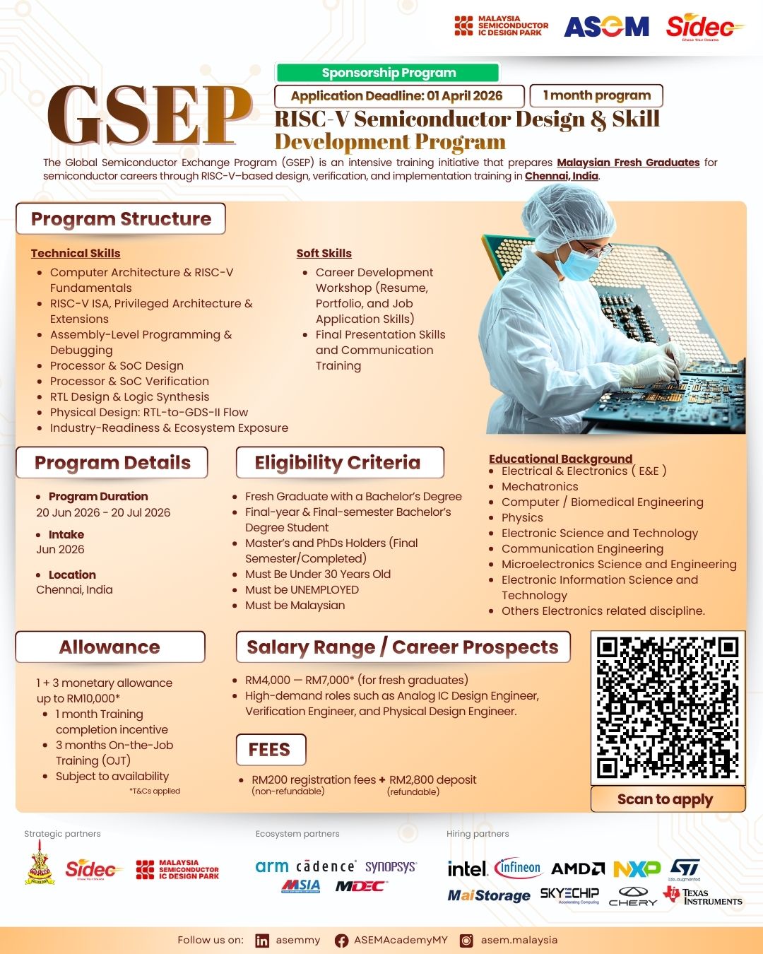
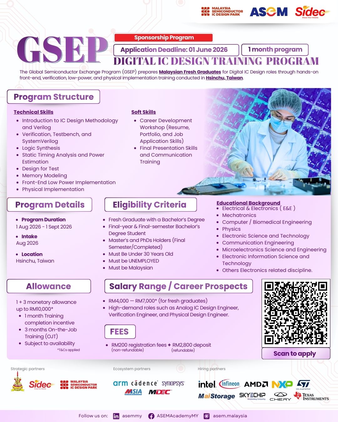
GSEP
Global Semiconductor Exchange Program
World-class training in Analog IC Design (China), Digital IC Design (Taiwan), and RISC-V Architecture (India), delivered through leading international partner institutions.
Gain global exposure. Build industry-ready expertise.
Open Now:
Analog IC Design (August 2026)
Registrations are closed
Course Details
FULL TIME
1 Month Classroom
3 Months On Job
Training
17 August-
16 December 2026
Allowances up to RM10,000
*Subject to T&C and Availability
ABOUT ASEM
Why Choose ASEM?
Industry-aligned courses in semiconductor IC design, test and packaging, and AI, to ensure students gain practical, job-ready skills.
Access to world-class labs and tools enhances learning, research, and industry readiness.
Partnerships with 100+ companies provide internships, collaborative projects, and direct job opportunities.
Clear pathways to high-demand, well-paying careers with strong job placement support.
International training and research collaborations with top institutions worldwide.
Contribute to Malaysia’s rise as a global tech leader while boosting academic and industry reputation.
K-Youth Development Programme
K-Youth Development Programme
The Khazanah Youth Development Programme (K-Youth) is a strategic youth employability initiative launched in 2023 by Khazanah Nasional Berhad to cultivate Malaysia’s next generation of talent. Designed to equip final-year students and fresh graduates with commercially relevant skills and hands-on experience, the program aims to enhance their employability within an evolving job market. K-Youth reflects a commitment to fostering innovation, creativity, and entrepreneurship, aligning with the “A Nation that Creates” framework and Malaysia MADANI aspirations to contribute meaningfully to the country’s long-term economic growth
Eligibility
Eligibility Criteria
Who Can Apply?
- Open to Malaysian only
- Degree holders in:
- Electronic & Electricals (E&E)
- Electronic Science and Technology
- Communication Engineering
- Microelectronics Science and Engineering
- Electronic Information Science and Technology
- Other electronics-related disciplines
- Unemployed Individual below age of 30
Screening Process
- Mini-Exam: Topics include Digital Logic, Analog Circuits, General Programming, and Semiconductor Electronics
- Online Interview: Candidates who pass the mini-exam will be received the link for an online interview.
Program Fees
- One time non-refundable admission fees of RM200
- A refundable deposit of RM2,800 is required
- All deposits will be fully refunded upon successful completion of the program and obtained full employment.
Pre-requisites / Requirements for GSEP Analog Design
- Semiconductor & Device Physics
- Basic Circuit Analysis
- MOS Device Physics
- Amplifier Design Knowledge
- Current Mirrors & Biasing
- Frequency Response Analysis
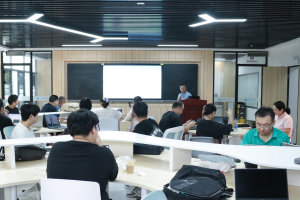
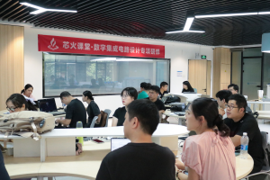
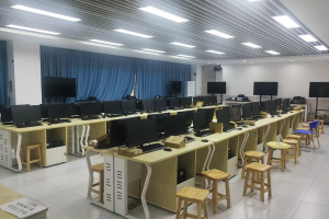
Training @ ASEM
Our GSEP Programmes
Registrations open
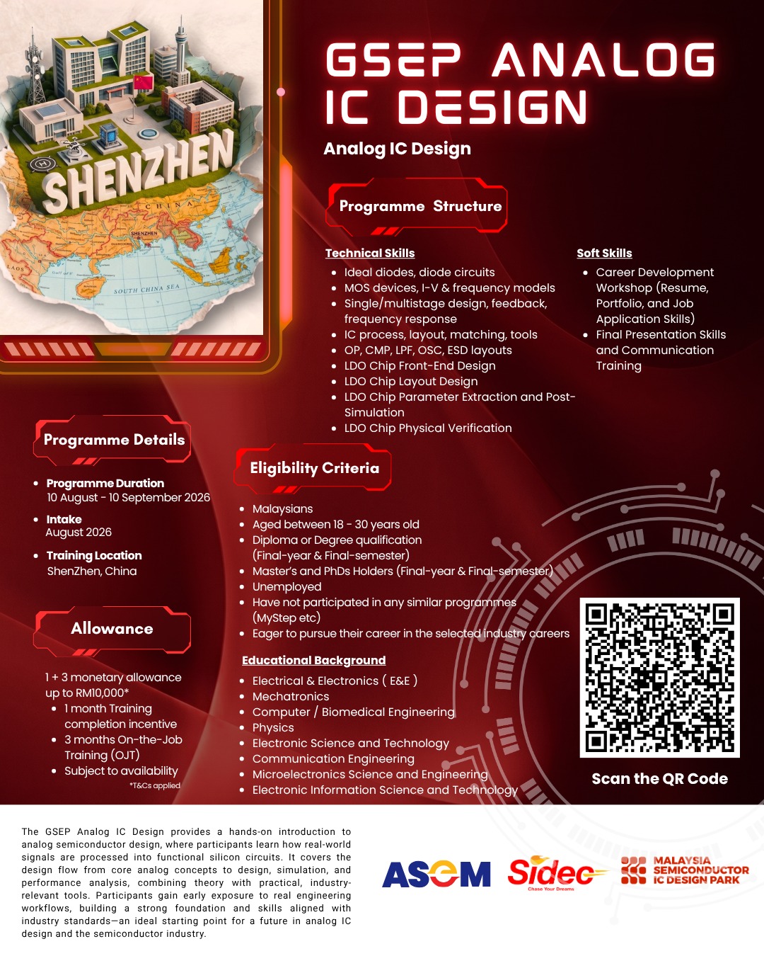
The GSEP programme at Shenzhen Institute of Information Technology (SZIIT) offers participants an immersive learning experience within one of the world’s most dynamic electronics and innovation ecosystems. Located in the heart of Shenzhen, the programme combines hands-on technical training with exposure to China’s advanced manufacturing, embedded systems, and hardware innovation landscape.
Participants will learn in well-equipped training facilities, engage with industry-relevant technologies, and gain first-hand insight into how engineering concepts are applied at scale in a real-world, high-velocity technology environment.
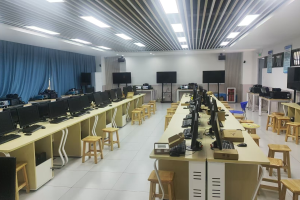
Venue & Facilities
Shenzhen Information Vocational Technology College, China
Batch Size: 30 Participants


What you'll learn
Core operation of analog components including diodes, MOS transistors, and amplifiers
Analog circuit analysis using large- and small-signal models, frequency response, and feedback
IC layout design fundamentals, including layout flow, matching techniques, and verification tools
Advanced analog layout practices for OP, CMP, LPF, OSC, and ESD circuits
End-to-end chip-level design through an LDO project, from schematic to layout and verification
Readiness for real-world IC design through integrated assessment and final evaluation
Course Modules
Analog Design
Core principles of analog IC design focusing on device behavior, circuit analysis, and amplifier architectures.
Key Topics
Device Fundamentals: Diodes, MOS structure, I–V characteristics, modeling
Signal Analysis: Large-signal and small-signal models, frequency behavior
Amplifier Design: Single & multi-stage amplifiers, feedback, output stages
Practical Exposure
Circuit analysis and design exercises
Simulation-driven validation
Layout Design
Hands-on exposure to analog IC layout methodologies and verification workflows.
Key Topics
Phase 1 – Layout Fundamentals:
IC process overview, layout flow, matching techniques, layout toolsPhase 2 – Advanced Layout Practice:
OP amp, CMP, LPF, OSC, and ESD protection layout design
Practical Exposure
Tool-based layout implementation
Design verification and practice-based learning
Final Project
An end-to-end capstone project integrating design, layout, and verification skills.
Key Topics
LDO chip front-end design
Layout implementation and extraction
Post-simulation and physical verification
Outcome
Complete LDO IC design project
Design review and technical presentation
Potential Career Paths
- Analog IC Design Engineer
- Mized-Signal IC Design Engineer
- Analog Layout Engineer
- Junior AMS Design Engineer
Registrations open
The GSEP programme at Indian Institute of Technology Madras (IIT Madras) provides participants with exposure to a leading academic and research-driven engineering ecosystem. Set within one of India’s top technical institutions, the program emphasises strong engineering fundamentals, system-level thinking, and application-oriented learning across electronics, computing, and semiconductor-related domains.
Participants will engage in structured technical sessions, learn within a rigorous academic environment, and gain insight into how advanced engineering research and industry collaboration shape real-world technology development.
Venue & Facilities
Indian Institute of Technology (IIT) Madras
Batch Size: 60 Participants
What you'll learn
Strong foundations in computer architecture and the RISC-V instruction set architecture (ISA)
Hands-on experience in processor and SoC design and verification using the IITM-Shakti infrastructure
Practical understanding of industry-standard RTL-to-GDSII physical design flows
Skills aligned with emerging semiconductor industry needs across design, verification, and implementation
Course Modules
Computer Organization and Architecture
Focus: System-level understanding
Ice-breaker and program orientation
Computer Organization and Architecture fundamentals
Processor components, datapath, and control concepts
Format: Lecture & case studies
RISC-V ISA and Assembly Programming
Focus: Instruction-level understanding
RISC-V ISA overview and design principles
Assembly programming and instruction execution
Hands-on exercises with RISC-V toolchains
Format: Lecture & hands-on sessions
Processor and SoC Designs & Verification
Focus: RTL design and verification
RISC-V processor microarchitecture
RTL implementation and verification concepts
Processor and SoC-level integration
Format: Lecture & hands-on sessions
Physical Design (RTL to GDS-II) Flow
Focus: Implementation and closure
RTL-to-GDSII physical design flow
Synthesis, placement, routing, and sign-off concepts
Practical exposure to industry workflows
Format: Lecture & hands-on sessions
Potential Career Paths
- RTL/Processor Design Engineer
- SoC Design Engineer
- Verification Engineer (Processor/SoC)
- Junior Hardware Architect
Timeline
Your Registration Timeline
Apply to your programme of choice
Submit your application by selecting your preferred programme and completing the required details.
What to expect next:
Eligible applicants will be shortlisted for the entrance examination
Demonstrate your fundamentals
Shortlisted candidates will receive and exam link via email. The assessment evaluates core technical fundamentals relevant to your chosen programme.
What to expect next:
Results will be reviewed, and successful candidates will proceed to the offer stage.
Confirm your placement
Qualified applicants will receive a Letter of Offer via email. This confirms your placement and includes key details on the programme structure and next steps.
Action required:
Accept the offer within the stated timeline to secure your slot.
Prepare for your learning journey
Once confirmed, you'll receive onboarding details including schedules, preparation guidelines, and communication channels.
You're officially in.
Get ready to begin your training and industry exposure.
Frequently Asked Questions
GSEP FAQs
- Q: What expenses are covered and sponsored for the GSEP program?
A: The program covers the training course, round-trip flight tickets, accommodation at the university, meals (three per day, seven days a week), and a visa. (Passport fees are not included.)
- Q: Are there any allowances?
A: Allowances are provided in collaboration with the K-Youth program up to RM10,000.
- Q: What is the process for obtaining a visa?
A: We will assist with the visa application process. If required, you must be available to visit the Embassy with us at least six weeks before the departure date. Please ensure your passport is ready and remains valid for at least six months beyond the program's end date. For example, if the program ends in July 2025, your passport should be valid until at least February 2026.
- Q: What is the application process for GSEP?
A: Applicants must first sign up via the provided form. They will then be scheduled for an exam, and those who pass will proceed to an interview.
- Q: What does the mini exam include, and how should we prepare?
A: The mini exam consists of both objective and subjective questions, covering fundamental topics in IC Design with Test and Verification.
- Q: How will the interview be conducted?
A: The interview will be held online as a group interview. During this session, we aim to learn more about you, including your educational background, job-seeking status, passion for the field, leadership roles in projects, and overall communication skills. Additionally, we will assess your commitment to full attendance throughout the program.
- Q: On which days do we need to attend the programme? Is it only on weekdays or does it include weekends?
A: The programme will be conducted on weekdays only. However, if a public holiday falls on a weekday, a replacement session may be scheduled on a weekend if necessary.
- Q: Will job placement be provided after completing the training and what is the process?
A: Yes, we will assist with job placement. You will need to apply for your desired job through our job portal, and we will forward your application to the respective company.
- Q: If I am shortlisted by an employer, do I still need to attend their interview even though I have already interviewed with ASEM?
A: Yes, you must attend the employer’s interview for job placement. The interview conducted by ASEM is solely for admission into the training program and selecting top candidates.
- Q: If I am not selected for this intake, can I apply for another intake or a different programme? Will I need to retake the exam and interview?
A: Yes, you can apply for a new intake or a different programme. Whether you need to retake the exam and interview will depend on the specific programme you are applying for and the intake you are joining, as programme modules and enrollment requirements may change.
Applications are now closed.
Thank you for your interest in our GSEP programs!
GSEP applications are currently closed. Register your interest to stay updated on future intake opportunities, or explore NSEP for upcoming local semiconductor training programs.
Enroll